A Deep Dive into the ARM Debug Access Port
Guest post
Exploring the Architecture and Capabilities of the ARM Debug Access Port for Embedded System Debugging
The ARM Debug Access Port (DAP) is a crucial component of the ARM debugging architecture that allows developers to gain access to and debug embedded systems running on ARM-based processors. The DAP provides a standardized interface for accessing and controlling various debug-related features, including debugging and programming interfaces, trace data, and system registers. Whether you are a seasoned embedded systems developer or just getting started with ARM-based SoC development, this article will provide valuable insights into the architecture of the ARM Debug Access Port and its functionality.
Table of Contents
Debug Access Port Architecture
The DAP is the primary “unit” of the ARM Debug Interface (ADI). DAP is a module that contains a set of registers and logic required to provide microcontroller debugging via a debug interface. DAP consists of two main components: Debug Port (DP) and Access Port (AP).
The Debug Port provides control of the DAP and establishes a connection between the debugger and the target device. DP performs functions such as initialization, reset, and operation status checking. This module is conditionally divided into two parts: common and specific to a particular debugging protocol. The common part contains registers used to configure and operate the DP module, and the specific part is responsible for working with external debugging protocols. According to the documentation, our microcontroller supports two debugging protocols: SWD and JTAG, but in this series of articles, I decided to choose JTAG for consideration. Therefore, in the future, unless specifically stated otherwise, I will describe the operation of DAP specifically in the context of the JTAG protocol.
The Access Port provides access to various resources of the microcontroller, such as memory. The Access Port can have several data exchange interfaces, such as APB (Advanced Peripheral Bus), AHB (Advanced High-performance Bus), and AXI (Advanced eXtensible Interface), which are used to access various device resources. That is, access to all modules connected to the AHB bus, for example, will be provided through a special AHB-AP.
The approximate structural diagram of DAP is shown in the following figure:
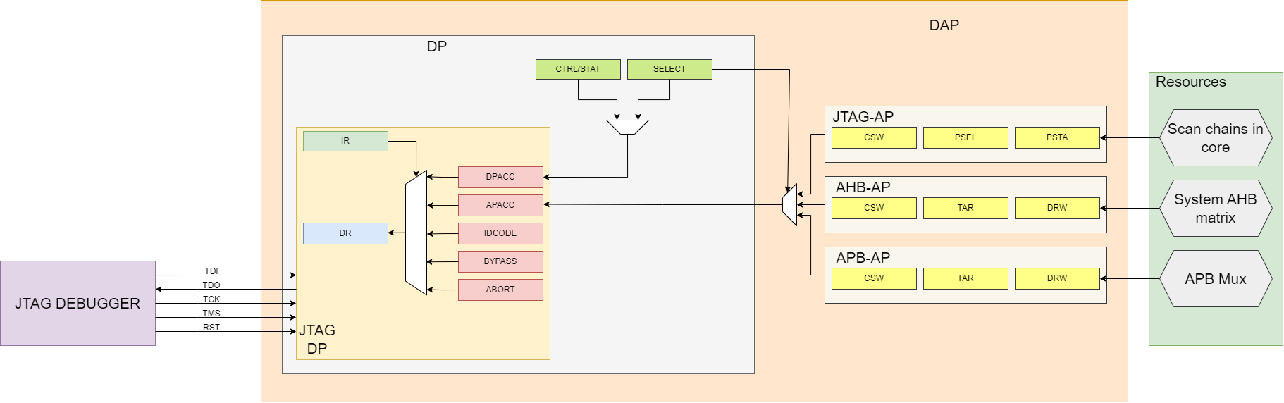
Figure 1 - Debug Access Port (DAP)
Now let’s consider each component of DAP shown on this block diagram.
Debug Port (DP)
JTAG Debug Port (JTAG-DP)
Since JTAG-DP must support the operation of the microcontroller via the JTAG protocol, external connection is made through the JTAG standard pins:
| JTAG-DP pin | JTAG pin | Direction | Description |
|---|---|---|---|
| DBGTDI | TDI | INPUT | Debug Data In |
| DBGTDO | TDO | OUTPUT | Debug Data Out |
| TCK | TCK | INPUT | Debug Clock |
| DBGTMS | TMS | INPUT | Debug Mode Select |
| DBGTRSTn | TRST | INPUT | Debug TAP Reset |
The JTAG-DP wire-level interface is through scan chains and comprises:
a Debug TAP State Machine (DBGTAPSM) - This state machine is the cornerstone of the JTAG protocol and will be discussed in detail in the next article dedicated to this protocol.
an Instruction Register (IR) and associated IR scan chain, used to control the behavior of the JTAG-DP and the currently-selected data register. The specific data register we want to work with is selected by writing various commands to this register.
several Data Registers (DRs) and associated DR scan chains.
JTAG Registers
Instruction Register (IR)
The Debug TAP State Machine is implemented with a 4-bit instruction register (IR).
The Instruction Register contains the current command for the DAP controller. This register serves as a kind of entry point when working with DAP over the JTAG protocol. You need to write a command to this register that will determine the data register you want to work with.
The list of commands for the IR register is presented in the following table:
| IR instruction value | DR name | DR length | Description |
|---|---|---|---|
| b1000 | ABORT | 35 | JTAG-DP Abort Register |
| b1010 | DPACC | 35 | JTAG-DP DP Register |
| b1011 | APACC | 35 | JTAG-DP AP Register |
| b1110 | IDCODE | 32 | Device ID Code Register |
| b1111 | BYPASS | 1 | JTAG-DP Bypass Register |
ABORT Instruction
The ABORT command in JTAG-DP is used to interrupt the execution of the current debugging operation and return control to the debugger. It allows performing a so-called debug reset of the processor.
During the debugging of a processor, the debugger establishes a connection with JTAG-DP and sends commands to read and write registers, execute instructions, etc. In some situations, there may be a need to interrupt the execution of the current debugging operation and return control to the debugger.
For example, in case of program hang or when there is an error in the debugging script. In such situations, the debugger can use the ABORT register to perform a debug reset of the processor and return control to the debugger.
BYPASS Instruction
The BYPASS command connects the TDI and TDO pins directly through a one-bit register called BYPASS. This command can be used to bypass some components connected to the JTAG chain. It may not be very clear now, but this command is closely related to the operation principle of the JTAG protocol and it’s difficult to explain it without discussing this principle. The next article will be dedicated to the JTAG protocol, so let’s postpone the explanation of this command for now. It’s not necessary for understanding the information in the current article.
IDCODE Instruction
The IDCODE command is used to identify the microchip connected to the JTAG chain. This command connects the IDCODE register, which contains a unique 32-bit identifier for the microchip, as the data register.
Reading the IDCODE register can be useful for verifying that the microchip corresponds to the expected model or version, as well as for checking the integrity and proper functioning of the JTAG chain.
DPACC Instruction
The DPACC command connects the 35-bit DPACC (Debug Port Access) register as the data register, which is used to access some Debug Port registers.
APACC Instruction
The APACC command connects the 35-bit APACC (Access Port Access) register as the data register, which is used to access registers of the selected Access Port.
Data Register (DR)
The Data Register is a JTAG register through which all communication with one of the five registers listed in Table 1 occurs. In other words, by specifying the code of one of the five registers in the IR register, you are connecting the DR register to the selected register and any read or write operation to the DR register will be mapped to the selected register.
Debug Port Registers
The DP is responsible for configuring the debug module, controlling power and reset, and monitoring various errors that may occur during DAP operation. Special registers, such as ABORT, IDCODE, CTRL/STAT, and SELECT are responsible for all of these tasks.
Abort Register (ABORT)
The Abort Register is always present on all DP implementations. Its main purpose is to force a DAP abort.
| Bits | Access | Function | Description |
|---|---|---|---|
| [1:31] | RO | - | Reserved |
| [0] | WO | DAPABORT | Write 1 to this bit to generate a DAP abort. This aborts the current AP transaction. Do this only if the debugger has received WAIT responses over an extended period. |
When working with this register within JTAG-DP, the only writable bit is the DAPABORT bit. Writing to the other bits of this register results in undefined behavior according to the documentation.
ID Code Register (IDCODE)
The Identification Code Register is always present on all DP implementations. It provides identification information about the ARM Debug Interface.
| Bits | Access | Function | Description |
|---|---|---|---|
| [31:28] | RO | Version | Version code |
| [27:12] | RO | PARTNO | Part Number for the JTAG-DP - 0xBA00 |
| [11:1] | RO | DESIGNER | JEDEC Designer ID, an 11-bit JEDEC code that identifies the designer of the ADI implementation - 0x23B |
| [0] | RO | - | Always |
Control/Status Register (CTRL/STAT)
The CTRL/STAT register is always present on all DP implementations. It provides control of the DP and status information about the DP.
| Bits | Access | Function | Description |
|---|---|---|---|
| [31] | RO | CSYSPWRUPACK | System power-up acknowledge |
| [30] | R/W | CSYSPWRUPREQ | System power-up request |
| [29] | RO | CDBGPWRUPACK | Debug power-up acknowledge |
| [28] | R/W | CDBGPWRUPREQ | Debug power-up request |
| [27] | RO | CDBGRSTACK | Debug reset acknowledge |
| [26] | R/W | CDBGRSTREQ | Debug reset request |
| [25:24] | - | - | Reserved, RAZ/SBZP |
| [23:12] | R/W | TRNCNT | Transaction counter |
| [11:8] | R/W | MASKLANE | Indicates the bytes to be masked in pushed compare and pushed verify operations |
| [7] | RO | WDATAERR | Set if a Write Data Error occurs |
| [6] | RO | READOK | This bit is set to 1 if the response to the previous AP or RDBUFF read was OK |
| [5] | RO | STICKYERR | Set if an error is returned by an AP transaction |
| [4] | RO | STICKYCMP | This bit is set to 1 when a match occurs on a pushed compare or a pushed verify operation |
| [3:2] | R/W | TRNMODE | Transfer mode for AP operations: 00 = Normal operation, 01 = Pushed verify operation, 10 = Pushed compare operation, 11 = Reserved. |
| [1] | RO | STICKYORUN | Overrun error flag |
| [0] | R/W | ORUNDETECT | This bit is set to 1 to enable overrun detection |
Let’s take a closer look at the bits of this register.
Sticky flags and DP error responses
A read or write error might occur within the DAP, or come from the resource being accessed. In either case, when the error is detected the Sticky Error flag, STICKYERR, in the CTRL/STAT Register is set to 1. A read/write error also might be generated if the debugger makes an AP transaction request while the debug power domain is powered down.
If a debugger issue APACC too fast, overrun may happen, the DP can be programmed so that if an overrun error occurs, the DP set the STICKYORUN flag in the CTRL/STAT register. But if overrun detection is on, the debugger must check for overrun errors after each sequence of APACC transactions, the DP will also no longer send FAULT response and WAIT response.
In any case, if a debugger receives a FAULT response from the DP, it must read the CTRL/STAT register to check the sticky flags.
The transaction counter
The DP includes an AP transaction counter, TRNCNT, which enables a debugger to make a single AP transaction request to generate a sequence of AP transactions, thus accelerating code download or memory fill operations. The TRNCNT maps onto the CTRL/STAT[23:12] bitfield, and writing a value N (N>=0) to this field generates N+1 AP transaction(s). If TRNCNT is not zero, it is decremented after each successful transaction, but it is not decremented when there are any sticky flags set. When reaches zero, TRNCNT does not auto-reload.
Power control
This is to enable an external debugger to connect to a potentially turned-off system and power up as much as required to get a basic level of debug access with a minimal understanding of the system.
The DAP model supports multiple power domains; there can be three power domains:
- Always on domain
- System power domain
- Debug power domain
The DP registers reside in the always-on domain, and there are two control bits in the CTRL/STAT register:
- Bit [28],
CDBGPWRUPREQ, used to request the system’s power manager to fully power up and enable clocks in the debug power domain. - Bit [30],
CSYSPWRUPREQ, used to request the system’s power manager to fully power up and enable clocks in the system power domain.
Debug Reset Control
The DP CTRL/STAT register provides bits [27:26], for reset control of the debug domain. The debug domain controlled by these signals covers the internal DAP and the connection between the DAP and the debug components, for example, the debug bus. The two bits provide a debug reset request, CDBGRSTREQ, and a reset acknowledge, CDBGRSTACK, and the associated signals provide a connection to a system reset controller. The DP registers are in the always-on power domain on the external interface side of the DP. Therefore, the registers can be driven at any time, to generate a reset request to the system reset controller.
AP Select Register, SELECT
The AP Select Register is always present on all DP implementations. Its main purpose is to select the current Access Port (AP) and the active four-word register bank within that AP.
| Bits | Function | Description |
|---|---|---|
| [31:24] | APSEL | Selects the current AP (AHB-AP, APB-AP, JTAG-AP) |
| [23:8] | - | Reserved |
| [7:4] | APBANKSEL | Select the active four-word register bank on the current AP |
| [3:1] | - | Reserved |
| [0] | - | Always |
AP selection
As DAP can contain multiple APs, we need to have the ability to select a specific AP with which we want to work at the moment. And it is the APSEL bits that are responsible for this selection. They specify the number of the AP that will be used for access.
Bank of registers selection
The APBANKSEL bits are used to select the register bank to which access will be made. Register banks are used to organize registers associated with specific functional blocks within the microcontroller. For example, a register bank may be allocated for the core processor debug registers, while another bank may be allocated for the peripheral device debug registers.
Accessing the DP registers
As mentioned earlier, to access the DP registers CTRL/STAT and SELECT, the DPACC register is used, and working with this register has its own peculiarities. Let’s take a closer look at the algorithm for accessing the DP registers.
DP registers can be divided into two categories: control registers and access registers. Control registers contain information about the state of the debug logic, such as the status of command execution or the reset state. Access registers are used to read and write data from registers that control the operation of the debug logic.
In this context, we will focus on the DP access registers, which provide access to the debug logic. DP access registers can be addressed through the DPACC register and include control registers (CTRL/STAT and SELECT), access registers to the application logic (APACC), bypass register (BYPASS), and device identification register (IDCODE). Working with these registers has its own peculiarities and requires knowledge of the DPACC register format, which we will discuss further.
DPACC register format
The DPACC register has a size of 35 bits and its format depends on the operation (read or write) we want to perform.
Format for writing:

Picture 2 - DPACC register write format
- D - these are data bits. That is, in these 32 bits, you store the value you want to write to the selected register.
- A - these are address bits of the DP register. These two bits determine the specific DP register you want to work with:
| Address | A[3:2] | Register |
|---|---|---|
| 0x04 | [01] | CTRL/STAT |
| 0x08 | [10] | SELECT |
- RnW - this bit for the write operation has the value 0.
Format for reading:

Picture 3 - DPACC register read format
- D - these are data bits. I.e. in these 32 bits you get the value read from the register.
- ACK[2:0] - Acknowledge of read operation:
| ACK | Value |
|---|---|
| 0b010 | OK/FAULT |
| 0b001 | WAIT |
Operation algorithm
Now let’s step by step go through the algorithms for writing/reading a new value to/from the DP register:
Algorithm for writing
- Write the value
0b1010(the code for theDPACCregister) to theIRregister. - Write 35 bits to the
DRregister according to the format described above:- DATA[31:0] - the data we want to write
- A[3:2] - the selected register
- RnW -
0b0
Algorithm for reading
- Write the value
0b1010(the code for theDPACCregister) to theIRregister. - Write a request to read the register to the
DRregister:- DATA[31:0] -
0x00 - A[3:2] - the selected register
- RnW -
0b1
- DATA[31:0] -
- Read 35 bits from the
DRregister:- DATA[31:0] - the data read from the register
- ACK[2:0] - Acknowledge code.
Access Ports
Access ports provide access to system resources such as debug registers, trace port registers, a ROM table, or system memory.
An ARM Debug Interface always includes at least one Access Port and might contain multiple APs. The simplest ARM Debug Interface uses a single AP to connect to a single debug component.
Multiple APs can be added to the DAP, depending on the needs. ARM provides specifications for two APs :
- Memory Access Port (MEM-AP). This AP provides access to the core memory and registers.
- JTAG Access Port (JTAG-AP). This AP allows to connect a JTAG chain to the DAP.
For this series of articles, the Memory Access Port is of the greatest interest, so we will focus on it. For information about the JTAG Access Port, please refer to the documentation.
Memory Access Port Registers
The specification for ARM DAP describes the following Memory Access Port registers:
| MEM-AP register | Address | Register bank (APBANKSEL) | Offset (A[3:2]) |
|---|---|---|---|
| CSW | 0x00 | 0x00 | 0b00 |
| TAR | 0x04 | 0x00 | 0b01 |
| DRW | 0x0C | 0x00 | 0b11 |
| BD0 | 0x10 | 0x01 | 0b00 |
| BD1 | 0x14 | 0x01 | 0b01 |
| BD2 | 0x18 | 0x01 | 0b10 |
| BD3 | 0x1C | 0x01 | 0b11 |
| CFG | 0xF4 | 0x0F | 0b01 |
| BASE | 0xF8 | 0x0F | 0b10 |
| IDR | 0xFC | 0x0F | 0b11 |
Control/Status Word Register, CSW
The CSW register is used to configure the access mode to the memory and peripheral devices of the ARM microcontroller.
Using the CSW register, you can configure parameters such as the size of the transmitted data (8, 16, or 32 bits), enable the auto-increment mode of the memory address to which access is made, and so on.
The Transfer Address Register (TAR)
This register is used to specify the address to be accessed through the AP. This address can be the address of a register, memory, or any other available address on the device.
When a new value is set in TAR in the AP, all subsequent read/write operations will be performed at the specified address until TAR is changed to another address and the auto-increment mode is turned off.
In general, before accessing any address through the AP, it is necessary to load this address into the TAR.
The Data Read/Write Register (DRW)
The DRW (Data Register for Write) in the Access Port is used for writing data to or reading data from the target resource.
To write data to DRW, the address needs to be set in the TAR (Transfer Address Register), and the necessary access parameters need to be configured in CSW. After that, data can be written to DRW and transferred to the target resource. Similarly, to read data from the target resource, the access parameters in CSW need to be configured and the read address needs to be set in TAR. Then, the data from the target device will be transferred to DRW, ready to be read.
Banked Data Registers 0 to 3 (BD0 to BD3)
The BD0, BD1, BD2 and BD3 registers in the Access Port are used for transferring/receiving data between the target device and the debugging system.
Using these registers can be useful when a large amount of data needs to be transferred or when a higher data transfer speed is required than what is possible with the TAR and DRW registers. Together, these four Banked Data Registers provide access to four words of memory space, starting at the address specified in the TAR. However, transferring data through the BD0, BD1, BD2 and BD3 registers requires more complex logic than transferring through the TAR and DRW registers and may require additional software to manage these registers.
Configuration Register (CFG)
The CFG Register holds information about the configuration of the MEM-AP. In particular, it indicates whether accesses to the connected memory system are big-endian or little-endian.
Debug Base Address Register (BASE)
The BASE Register is a pointer to the connected memory system. It points to one of: - the start of a set of debug registers for the single connected debug component - the start of a ROM Table that describes the connected debug components
Identification Register (IDR)
The IDR identifies the Memory Access Port. The IDR is the only register that must be implemented by any Access Port.
Addressing of AP Registers
One of the four registers within the DP is the AP Select Register (SELECT). This register specifies a particular Access Port and a bank of four 32-bit words within the register map of that AP.
In any AP access transaction from the debugger, the two address bits A[3:2] are decoded to select one of the four 32-bit words from the register bank indicated by the SELECT register (see Table 9). In other words, they select a specific register within the selected four-register bank.
This access model is shown in Figure 4 shows how the contents of the SELECT register are combined with the A[3:2] bits of the APACC scan-chain to form the address of a register in an AP.
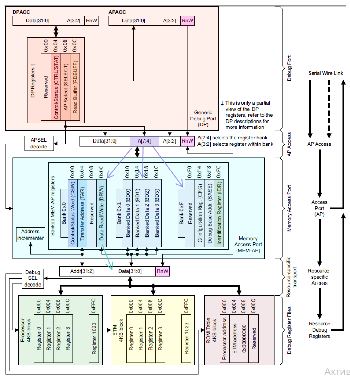
Figure 4 - MEM-AP access model
As can be seen in this figure, Memory Access Port registers are all 32-bit long (4 bytes), two fields in the DP SELECT register select the AP (APSEL field) and the register bank in the AP (APBANKSEL field), and finally, the A[3:2] field of APACC specify the exact AP register in the bank.
Accessing the AP registers
The situation with accessing the AP registers is the same as accessing the DP registers, except that instead of the DPACC register, the APACC register is used. When you write APACC command in the IR register, the DR register is mapped to the APACC register and the APACC register is mapped to one of the common AP registers defined in Table 9. This creates a chain of registers: DR --> APACC --> AP Reg.
APACC register format
These registers also have a size of 35 bits, and the value of the bits depends on whether we write something to these registers or read from them.
Format for writing:
Figure 5 - APACC register write format
- D - This is the data bits. In these 32 bits, you store the value that you want to write to the selected register.
- A - These are the sub-address bits of the AP register. These two bits, together with four more bits from the DP register
SELECT, determine the specific AP register you want to work with:
| Address | A[3:2] | Register |
|---|---|---|
| 0x00 | [00] | CSW |
| 0x04 | [01] | TAR |
| 0x0C | [11] | DRW |
| 0x10 | [00] | BD0 |
| 0x14 | [01] | BD1 |
| 0x18 | [10] | BD2 |
| 0x1C | [11] | BD3 |
| 0xF4 | [01] | CFG |
| 0xF8 | [10] | BASE |
| 0xFC | [11] | IDR |
- RnW - This bit has a value of 0 for a write operation.
Format for reading:
Figure 6 - APACC register read format
- DATA[31:0] - These are data bits. In other words, these 32 bits contain the value that you read from the selected register.
Bits 2:0 (ACK[2:0]) = 3-bit Acknowledge of read operation:
- 0b010 = OK/FAULT
- 0b001 = WAIT
Operation algorithm
Now let’s go step-by-step through the algorithms for writing/reading a new value to/from an AP register:
Algorithm for writing
- Write the
DPACCcommand (0b1010) to theIRregister - Write 35 bits to the
DRregister in which we indicate that we are working with theSELECTregister and write the corresponding values of the APSEL[31:24] and APBANKSEL[7:4] bits to this register:- DATA [31:0]:
- APSEL[31:24] - select the desired AP
- APBANKSEL[7:4] - select the desired bank of registers
- A[3:2] -
0b10- address ofSELECTregister (see Table 7) - RnW =
0b0
- DATA [31:0]:
- Write the
APACCcommand (0b1011) to theIRregister - Write the data to the
DRregister according to the described bit values (see Figure 5):- DATA[31:0] = data which need to be written
- A[3:2] = Address of Memory Access Port register (see Table 9).
- RnW =
0b0
Algorithm for reading
- Write the
DPACCcommand (0b1010) to theIRregister - Write 35 bits to the
DRregister in which we indicate that we are working with theSELECTregister and write the corresponding values of the APSEL[31:24] and APBANKSEL[7:4] bits to this register:- DATA[31:0]:
- APSEL[31:24] - select the desired AP
- APBANKSEL[7:4] - select the desired bank of registers
- A[3:2] -
0b10- address ofSELECTregister (see Table 7). - RnW =
0b1
- DATA[31:0]:
- Write the
APACCcommand (0b1011) to theIRregister - Create the data read request. Write in
DRnext data:- DATA[31:0] =
0x00000000 - A[3:2] = Address of Memory Access Port register (see Table 9).
- RnW =
0b1
- DATA[31:0] =
- Read 35 bits from the
DRregister - Check the values of the ACK[2:0] bits and if they are not equal to
OK/FAULT (0b001), then the data was read, if it is equal toWAIT (0b001), we need to repeat the reading because the data is not ready.
Practical Part
Let’s take an example of an algorithm for writing values to the memory of a microcontroller and reading data from memory.
Writing a variable to memory
Let’s try to write the value 0xAA55AA55 to the memory cell at address 0x20000000
- Write
0b1010(theDPACCregister code) into theIRregister. - Some settings in the
APregisterCSWneed to be configured. To access this register, we need to select the correspondingAPand register bank in theDP SELECTregister. Write to theDRregister:- DATA[31:0] =
0x00- APSEL[31:24] =
0x00 - APBANKSEL[7:4] =
0x00
- APSEL[31:24] =
- A[3:2] =
0b10(address ofSELECTregister) - RnW =
0b0
- DATA[31:0] =
- Next, we need to write the
CSWregister. Since this is anAPregister, we need to use theAPACCregister to access it:- Write
0b1011(theAPACCregister code) into theIRregister.
- Write
- Form the data for the configuration: set the data size for writing to 32-bits (
Size[0:2] = 0b010), disable the auto-increment function of the address (AddrInc[5:4] = 0b00). Write toDR:- DATA[31:0] =
0x00000002 - A[3:2] =
0b00(address ofCSWregister) - RnW =
0b0
- DATA[31:0] =
- Then we need to set the address of the memory cell to which we want to write the data. This is done through the
APregisterTAR. And since this register belongs to the sameAPasCSWand is in the same bank, we can omit the reference to theDP SELECTregister and immediately write the address value. Write toDR:- DATA[31:0] =
0x20000000 - A[3:2] =
0b01(address ofTARregister) - RnW =
0b0
- DATA[31:0] =
- The last step is to actually write the data. To do this, we need to write them to the
DRWregister. Write toDRW:- DATA[31:0] =
0xAA55AA55 - A[3:2] =
0b11(address ofDRWregister) - RnW =
0b0
- DATA[31:0] =
Reading a variable from memory
We know how to write data to memory, and now it’s time to read that data. The algorithm for reading largely repeats the steps for writing, but there are still some differences:
- Write
0b1010(theDPACCregister code) into theIRregister. - We need to configure some settings in the
CSWregister of theAP. To access this register, we need to select the correspondingAPand register bank in theDP SELECTregister. Using the data from the table, we form 35 bits of data that we write to theDRregister:- DATA[31:0] =
0x00- APSEL[31:24] =
0x00 - APBANKSEL[7:4] =
0x00
- APSEL[31:24] =
- A[3:2] =
0b10(address ofSELECTregister) - RnW =
0b0
- DATA[31:0] =
- Next, we need to write directly to the
CSWregister. Since this is anAPregister, we need to use theAPACCregister to access it:- Write
0b1011(theAPACCregister code) into theIRregister.
- Write
- We form the data for configuration: we set the data size for writing to 32 bits (
Size[0:2] = 0b010) and disable the auto-increment address function (AddrInc[5:4] = 0b00). Write toDR:- DATA[31:0] =
0x00000002 - A[3:2] =
0b00(address ofCSWregister) - RnW =
0b0
- DATA[31:0] =
- Next, we need to set the address of the memory cell from which we will read the data. This is done through the
TARregister of theAP. And since this register belongs to the sameAPasCSWand is in the same bank, we can skip theDP SELECTregister access and immediately write the address value:- DATA[31:0] =
0x20000000 - A[3:2] =
0b01(address ofTARregister) - RnW =
0b0
- DATA[31:0] =
- We form a read request. To do this, we write to the
DRWregister:- DATA[31:0] =
0x00 - A[3:2] =
0b11(address ofDRWregister) - RnW =
0b1
- DATA[31:0] =
- Read the
DRWregister by reading 35 bits from theDRregister. - Check the values of the
ACK[2:0]bits, and if they are equal to0b001, the read operation is complete. However, to ensure that the read data is valid, we need to check for read errors. - To check error flags, we need to read the
CTRL/STATregister of theDPand, first of all, check theSTICKYERRflag.
Links
- ARM® Debug Interface v5. Architecture Specification
- A Deep Dive into ARM Cortex-M Debug Interfaces
- JTAG Implementation in Arm Core Devices
- AN115533 - Serial Wire Debug (SWD) programming specification
Stay in touch with us
Stay tuned to this blog or follow us on LinkedIn and Twitter @PlatformIO_Org to keep up to date with the latest news, articles and tips!