Basics of Wired Embedded Protocols
Guest post
A Comprehensive Look at the Physical Level Principles that enable Reliable Embedded System Communication
The essence of any protocol lies in the transmission of data. In the world of digital electronics, data is represented in binary form, that is, as sequences of zeros and ones. These two symbols form the foundation for storing, processing, and transmitting all information in digital systems, with protocols serving as the key tools for exchanging these binary data, providing a structured and reliable method of transferring them between devices.
Table of Contents
The concepts of a logical one and a logical zero play a central role in the architecture of digital electronics, creating the fundamental basis for all data operations. From simple logic gates that form the basic building blocks of electronic circuits to complex microprocessors and digital communication systems, these foundational concepts are employed everywhere.
Logical Zero typically represents the absence of voltage or a lower voltage level in an electronic circuit. In the context of the binary numeral system, a logical zero corresponds to the value “0”.
Logical One represents the presence of voltage or a higher voltage level. In the binary numeral system, a logical one corresponds to the value “1”.
However, in practice, these abstract concepts require specification. It is essential to clearly define which voltage levels correspond to logical zero and one and how these levels are transmitted in physical circuits. These aspects are fundamental for the design and utilization of any data transmission systems. In this chapter, we will delve into the details necessary for a deep understanding and effective work with wired data transmission protocols.
Voltage Levels
When we talk about logical one and logical zero, we often use relative terms: high or low level, presence or absence of a signal. However, in real circuits, these levels are represented by specific voltage values. In this section, we will examine how voltage is used to encode logical levels in various digital circuit technologies.
In typical digital circuits, logical one and logical zero are encoded using different voltage levels:
- Logical one usually corresponds to the full supply voltage.
- Logical zero corresponds to zero voltage or a voltage close to zero.
Ideally, signals in digital circuits would always adopt only these two levels: maximum supply voltage for logical one and zero for logical zero. However, in practice, various factors, such as parasitic effects, voltage drops across transistors, and noise, lead to deviations from these ideal values.
Despite this, digital circuits can correctly interpret signals by using voltage ranges within which values are defined as logical one or logical zero. In real circuits, the levels of logical one and zero are not single specific values but rather ranges of voltage values, where a signal falling within these ranges will be interpreted as either logical one or logical zero:
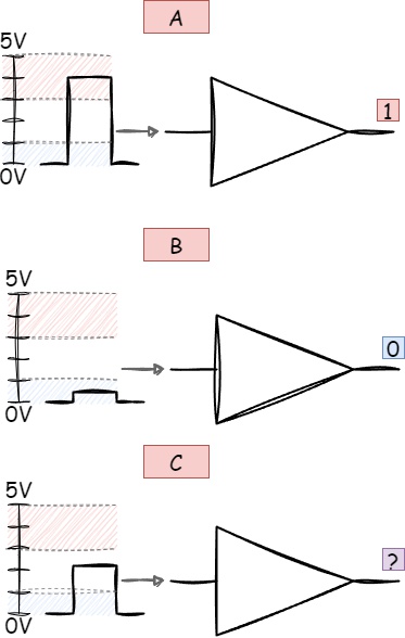
Figure 1.1 - Voltage ranges for interpreting 1 and 0
As we can see, the logical one and zero correspond to specific voltage ranges, marked in red for one and blue for zero. If the signal level falls within these ranges, the chip is guaranteed to correctly interpret the signal (sections A and B). However, there is a gap between these two ranges (section C), where the presence of a signal makes it impossible to interpret.
These voltage ranges are standardized based on the circuit technology used in the design of a particular chip. There are many such technologies: ECL (Emitter-Coupled Logic), RTL (Resistor-Transistor Logic), DTL (Diode-Transistor Logic), and so on. However, I will focus on two of the most well-known: TTL (Transistor-Transistor Logic) and CMOS (Complementary Metal-Oxide-Semiconductor).
Note 1: Currently, CMOS is the dominant technology for manufacturing most modern integrated circuits, including processors, memory, and mobile devices.
TTL (Transistor-Transistor Logic)
TTL (Transistor-Transistor Logic) is a technology developed and widely adopted in the 1960s, which became the foundation for many digital devices due to its reliability and design simplicity. As the name suggests, all logic elements in this technology are implemented using bipolar transistors.
Let’s look at an example of a two-input NAND gate constructed using TTL logic:
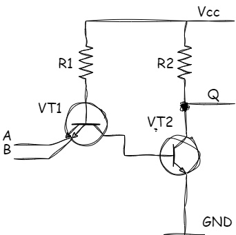
Figure 1.2 - Two-input TTL NAND gate
Components based on TTL logic are designed to operate with a standard supply voltage of 5 volts, with allowable variations within +/- 0.25 volts. Ideally, a signal corresponding to a high logical level would have a voltage exactly at 5 volts, and a signal representing a low logical level would be exactly 0 volts. However, in practice, TTL components can correctly interpret logical levels even when they deviate from these ideal values. Acceptable voltage ranges for input signals vary from 0 to 0.8 volts for a low level and from 2 to 5 volts for a high level. For output signals, manufacturers guarantee that, under certain load conditions, voltages will remain within 0 to 0.5 volts for a low level and 2.7 to 5 volts for a high level:
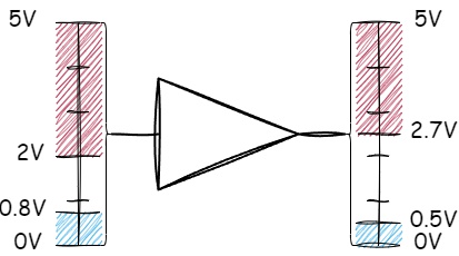
Figure 1.3 - Voltage ranges for TTL logic
When a signal with a voltage between 0.8 and 2 volts is applied to the input of a TTL element, no clear response from the circuit can be expected. Such a signal will be interpreted as undefined, and no manufacturer will provide guarantees as to which logical level it will be assigned.
You may notice that the allowable limits for output signal levels are stricter compared to those for input signals. This ensures that every digital signal transmitted from the output of one TTL element to the input of another corresponds to a voltage acceptable for the latter. This difference in tolerances for input and output signals is referred to as the noise margin (high or low level). In TTL logic, the noise margin for the low logical level is the difference between 0.8 V and 0.5 V (i.e., 0.3 V), and for the high logical level, it is the difference between 2.7 V and 2 V (i.e., 0.7 V). In other words, the noise margin determines the maximum allowable noise or interference that can be superimposed on the output signal of a logic circuit before the receiving circuit begins to misinterpret it.
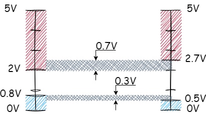
Figure 1.4 - Noise margin for TTL logic
If the allowable levels for input and output signals in TTL logic were the same, the system’s noise immunity would be significantly reduced. Any slight change in the output signal caused by external noise or interference could lead to that signal being misinterpreted at the input of the next element. In such a situation, the system would become extremely vulnerable to external influences, potentially causing a chain reaction of errors in the logic circuits, rendering reliable system operation nearly impossible.
The noise margin creates a “buffer” between the levels at which signals are considered valid, ensuring that signals subjected to minor changes due to noise are still correctly interpreted by the receiver. This is critically important for ensuring the reliability and stability of digital devices, especially in environments with high levels of electromagnetic interference.
CMOS (Complementary Metal-Oxide-Semiconductor)
The CMOS technology, widely adopted since the 1970s, uses pairs of complementary field-effect transistors (MOSFETs), including n-channel and p-channel transistors, to create efficient logic circuits. This technology achieves high energy efficiency because significant power consumption occurs only during state transitions of the circuit, while in a static state, power consumption is extremely low. This characteristic makes CMOS circuits ideal for portable devices where battery life is a critical concern.
Additionally, CMOS technology offers high noise immunity and the ability to operate within a wide range of supply voltages, extending its applications not only in portable electronics but also in various areas of digital technology, including computers, mobile phones, and consumer electronics. These features, combined with the capability to integrate a large number of transistors on a relatively small silicon substrate area, have made CMOS technology the dominant choice for manufacturing microprocessors, memory, and other integrated circuits.
The same two-input NAND gate implemented using CMOS logic would look as follows:
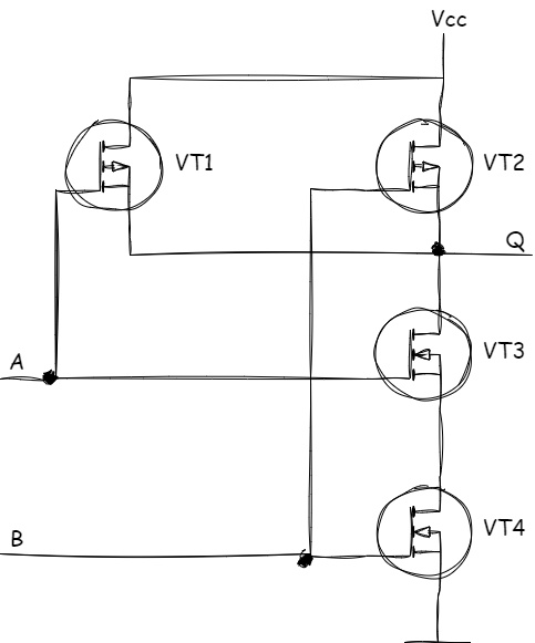
Figure 1.5 - Two-input CMOS NAND gate
Voltage levels for CMOS technology depend on the supply voltage, enabling these circuits to operate across a wide voltage range. This is one of the key advantages of CMOS, as it provides greater flexibility in designing electronic devices and systems. A typical range for CMOS supply voltages can vary from 1.8 V to 15 V.
Let us consider the voltage levels for CMOS logic with a supply voltage of 5V.
In the context of CMOS elements with a supply voltage of 5 volts, acceptable voltage levels for input signals range from 0 to 1.5 volts for a low logical level and from 3.5 to 5 volts for a high logical level. For output signals, manufacturers guarantee voltage levels between 0 and 0.05 volts for a logical zero and between 4.95 and 5 volts for a logical one:
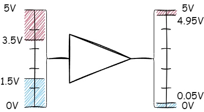
Figure 1.6 - Voltage ranges for CMOS logic
These voltage values illustrate that CMOS logic elements have significantly greater noise margins compared to TTL-based elements. The noise margin for CMOS is 1.45 volts for both logical zero and logical one, whereas for TTL, this margin reaches a maximum of 0.7 volts:
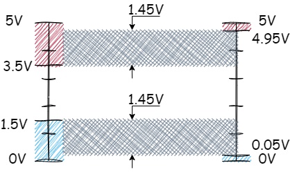
Figure 1.7 - Noise margin for CMOS logic
This means that CMOS circuits can tolerate more than double the amount of noise imposed on input signals without misinterpreting them as logical zeros or ones.
Pull-Up and Pull-Down Resistors
A pull-up resistor is a fundamental component in embedded system design, used to ensure a stable logical level on the input or output of a microcontroller or other digital logic when the input/output may be inactive or floating.
A pull-up resistor is connected between the corresponding input/output and the power supply voltage (VCC) or ground (GND). Its primary function is to “pull” the voltage level on the input/output to a high or low logical level when other active elements in the circuit are not influencing that input/output.
What does it mean to “pull”? It means that in the idle state of the line — when no device is transmitting on it — a specific signal level will be established: either logical one or logical zero. This is a crucial concept because such pulling ensures that we can always reliably determine the current signal level on the communication line.
Pull-up resistors serve the following purposes:
- Eliminating Floating States: Inputs on microcontrollers and other digital devices can “float” if they are not connected to a defined logical level. A “floating” input can randomly be interpreted as high or low due to electrical noise, leading to unpredictable behavior. Pull-up resistors ensure a stable logical state.
- Ensuring Correct Control Logic: In certain circuits, for example, when a button or switch is used to close a circuit to ground, a pull-up resistor ensures that the input remains high in the absence of activation and transitions to a low level only when the button is pressed.
- Reducing Noise: Maintaining an input or output in a defined state reduces susceptibility to electrical noise.
Pull-Up Resistors
Pull-up resistors are connected between the signal line and the positive power supply:
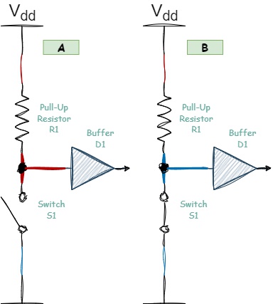
Figure 1.8 - Pull-Up Resistor
When the switch S1 is open (section A of Figure 1.8), the entire line is connected to the power supply through the pull-up resistor R1, and a high logical level is established on the line. If the switch S1 is closed (section B of Figure 1.8), it creates a direct connection to ground, and the logical level on the line changes to low.
Thus, this pull-up resistor ensures a high logical level on the line in an idle state. This type of pull-up resistor is crucial for our topic, as it is used in many protocols to pull signal lines up to the supply voltage. Without this resistor, the operation of these protocols cannot be organized. Examples of protocols that require the presence of a pull-up resistor include 1-Wire and I2C.
Pull-Down Resistors
Pull-down resistors are connected between the signal line and ground:
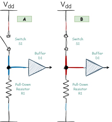
Figure 1.9 - Pull-Down Resistor
When the switch S1 is open (section A of Figure 1.9), the entire line is connected to ground through the pull-down resistor R1, and a low logical level is established on the line. If the switch S1 is closed (section B of Figure 1.9), it creates a direct connection to the power supply line, and the logical level on the line changes to high.
This type of pull-down resistor is not used in the protocols discussed in this book. However, it is frequently applied to ensure a stable logical zero level on the microcontroller pins. It is often used for all unused pins of a microcontroller.
Selecting the Resistor Value
The value of pull-up and pull-down resistors depends on the specific application. They must be large enough not to impose a significant load on the power supply circuit, yet small enough to ensure rapid changes in logical levels.
- Too low a resistance increases current consumption, which is especially critical for battery-powered devices.
- Too high a resistance can slow down signal transitions, reduce the signal-to-noise ratio, and increase susceptibility to interference.
Let’s take a closer look at the factors that influence the selection of the resistor value.
The Impact of Power Consumption on Resistor Selection
First, let’s examine the phrase: not to impose a significant load on the power supply circuit. A current flows through the pull-up resistor, as it does through any circuit element, and this current is drawn from the power source connected to the device. According to Ohm’s Law, the value of the pull-up resistor directly affects the current flowing through it, and consequently, the total current consumption of the entire circuit.
Note 2: Ohm’s Law states that the current (\(I\)) through a resistor is proportional to the voltage (\(V\)) across it and inversely proportional to its resistance (\(R\)): \(I = \frac{V}{R} \tag{1.1}\)
Let’s compare the current consumption for three cases of pull-up resistor values: 1 kΩ, 4.7 kΩ, and 10 kΩ, with a supply voltage of 5V:
- For a 1 kΩ resistor, the current value will be: \(I = \frac{V}{R} = \frac{5 (V)}{1000 (Ω)} = 5 (mA)\)
- For a 4.7 kΩ resistor, the current value will be: \(I = \frac{V}{R} = \frac{5 (V)}{4700 (Ω)} ≈ 1 (mA)\)
- For a 10 kΩ resistor, the current value will be: \(I = \frac{V}{R} = \frac{5 (V)}{10000 (Ω)} = 500 (\mu\text{A})\)
These values illustrate how current changes depending on the resistor’s resistance. The difference between the extreme values is up to 10 times, which is critical for low-power devices.
Increasing the resistance of the resistor reduces the current flowing through the circuit, which decreases power consumption — an essential factor for battery-powered devices. However, by reducing the current through higher resistance, you also weaken the signal, and a weak signal:
- Increases the likelihood of errors during data transmission due to the reduced signal amplitude relative to noise levels.
- Makes the line more susceptible to electromagnetic interference and parasitic capacitance.
Pull-up resistors are often chosen within the range of \(1\text{k}\Omega - 10\text{k}\Omega\). This range provides a reasonable trade-off between power consumption, switching speed, and data transmission reliability.
The Effect of Signal Speed on Resistor Value Selection
Now let’s take a closer look at the phrase: ensure rapid changes in logical levels.
The fact is that the signal line and ground create what is known as a parasitic capacitor — a data transmission line inherently has capacitance, even if no physical capacitor is connected. This capacitance arises due to the parasitic capacitance of PCB traces, cables (in the case of external devices), IC pins, and other components of electrical circuits, all of which inherently possess some level of capacitance. These capacitances occur both between signal conductors themselves and between power lines, signal conductors, and everything else on the board.
When you add the resistance of the pull-up resistor to this capacitance, an RC circuit is formed:
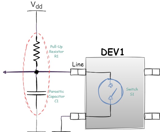
Figure 1.10 - RC circuit formed by a pull-up resistor and parasitic capacitance
The main characteristic of any RC circuit that affects the speed of signal changes is the time constant of the circuit (\(RC\) constant).
The \(RC\) constant time constant of a circuit is defined by the following formula:
\[\tau = R \cdot C \tag{1.2}\]where:
- \(\tau\) — the time constant of the circuit,
- \(R\) — resistance in ohms (Ω),
- \(C\) — capacitance in farads (F).
It is measured in seconds and represents the time required for the signal to reach approximately 63.2% of the full charge of capacitor \(C\) in response to a step change in voltage across resistor \(R\) from logical zero to logical one:
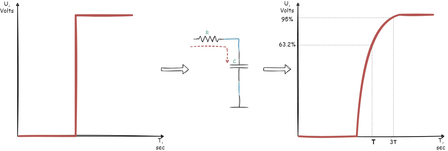
Figure 1.11 - The effect of the RC constant on capacitor charging
Or for the capacitor to discharge to 36.8% of its initial value in response to a step change in voltage across resistor \(R\) from logical one to logical zero:
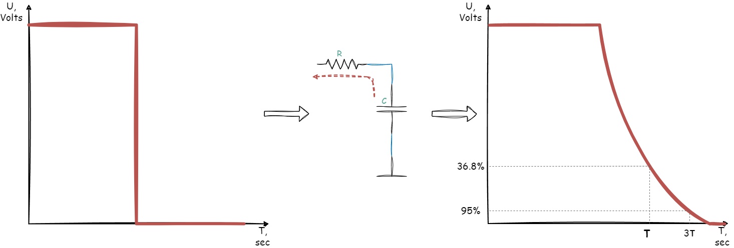
Figure 1.12 - The effect of the RC constant on capacitor discharging
Note 4: The formula \(\tau = R \cdot C\) is used for simplified circuit analysis. The time constant (\(\tau\)) represents the time required for the voltage across the capacitor to reach approximately 63% of the full charge level (\(V_{PULLUP}\)), and this formula is used as an approximation for rough calculations.
However, the charging process is described by the equation:
\[V(t) = V_{PULLUP} \cdot \left(1 - e^{-\frac{t}{R \cdot C}}\right) \tag{1.3}\]To determine the time required for the voltage to reach a specific level \(V(t)\) (different from 63% or 95%), this equation can be rearranged as:
\[t = -R \cdot C \cdot \ln\left(1 - \frac{V(t)}{V_{PULLUP}}\right) \tag{1.4}\]This is a more precise expression that describes the capacitor charging process, based on the exponential relationship of voltage over time.
However, for our purposes — understanding the reason for delayed signal edges — the formula \(\tau = R \cdot C\) is sufficient.
From formula \(1.2\), it follows that the higher the resistor’s resistance, the larger the value of \(\tau\), and thus the longer it takes for the signal to transition from one logical level to another. Consequently, the slower the protocol that can operate on this line.
Let’s again compare the values of \(\tau\) for the same three pull-up resistor values: 1 kΩ, 4.7 kΩ, and 10 kΩ, assuming a parasitic capacitance of 10 nF:
For a 1 kΩ resistor: \(\tau = R \cdot C = 1 \, \text{k}\Omega \cdot 10 \, \text{nF} = 0.00001 \, \text{s} = 10 \, \mu\text{s} \tag{1.5}\)
For a 4.7 kΩ resistor: \(\tau = R \cdot C = 4.7 \, \text{k}\Omega \cdot 10 \, \text{nF} = 0.000047 \, \text{s} = 47 \, \mu\text{s} \tag{1.6}\)
For a 10 kΩ resistor: \(\tau = R \cdot C = 10 \, \text{k}\Omega \cdot 10 \, \text{nF} = 0.0001 \, \text{s} = 100 \, \mu\text{s} \tag{1.7}\)
This parameter significantly affects the shape of the signal we actually observe on the line. Let’s explore how this happens in more detail.
Let’s take our circuit with a pull-up resistor and a switch, but this time connect an oscilloscope to it:
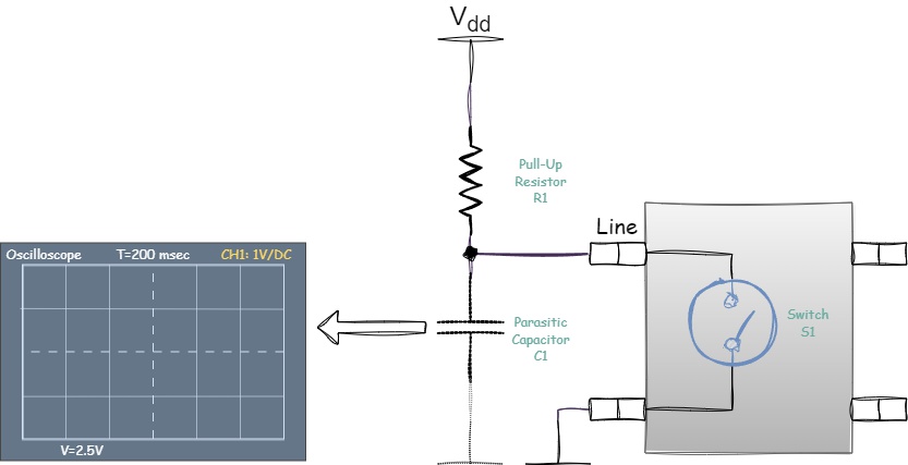
Figure 1.13 - Initial circuit for analyzing the effect of the RC constant on signal shape
We begin toggling the switch S1 at a fixed frequency. On the oscilloscope screen, we expect to see the following signal:
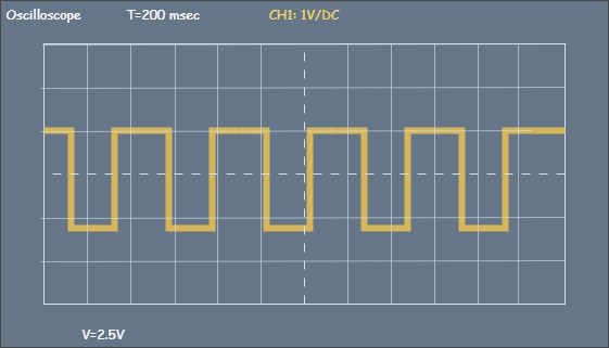
Figure 1.14 - Ideal signal shape
However, in reality, we might observe something like this:
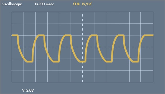
Figure 1.15 - Actual signal shape
This signal distortion occurs, as you might have guessed, due to the presence of parasitic capacitance and the formation of an RC circuit.
Let’s examine this in detail using a single signal period as an example.
When the switch S1 is open, parasitic capacitance starts charging through the pull-up resistor from the power line. The charging time depends on the value of the \(RC\) constant. On the oscilloscope screen, this will appear as a distorted signal:
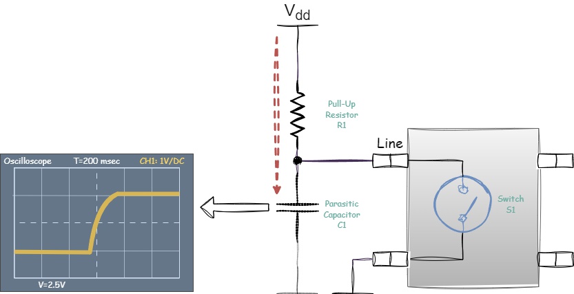
Figure 1.16 - Signal shape during the charging of parasitic capacitance
Now let’s close the switch S1. The parasitic capacitor starts discharging through the switch S1. Since it discharges directly through the switch and not through the resistor, the discharge process is faster than in a classic RC circuit, as shown in Figure 1.12. This is why the falling edge appears smooth. When the capacitor is fully discharged, the line reaches a low logical level:
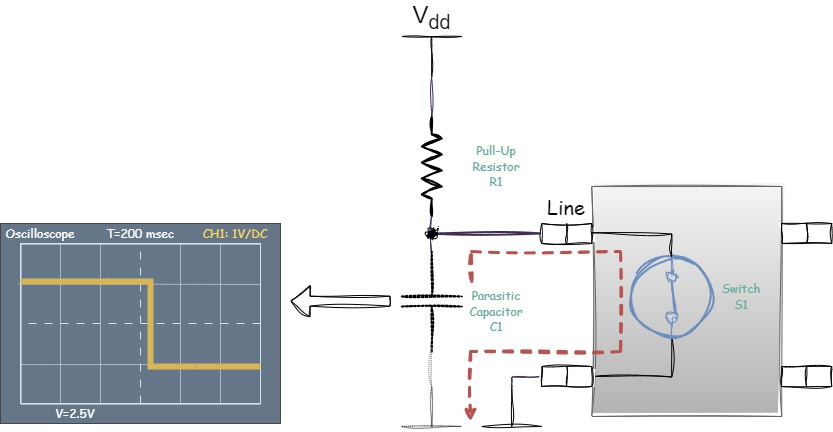
Figure 1.17 - Signal shape during the discharge of parasitic capacitance
This process repeats for every signal period, resulting in the following signal on the oscilloscope:
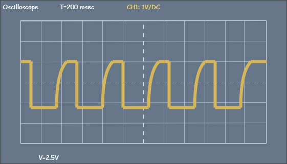
Figure 1.18 - Actual signal shape during capacitor charging/discharging
The greater the total parasitic capacitance, the more pronounced the distortion of the signal edges becomes. Since parasitic capacitance is often beyond our control, we must manage these distortions by adjusting the resistance of the pull-up resistor.
The main issue here is that parasitic capacitance and the RC circuit delay the signal edges, which severely limits the maximum frequency at which signals can be transmitted on the line. If this delay is too long, the signal may fail to reach the required voltage level for the IC to unambiguously interpret the input signal as a 1. Let’s illustrate this using an example of an IC with CMOS voltage levels.
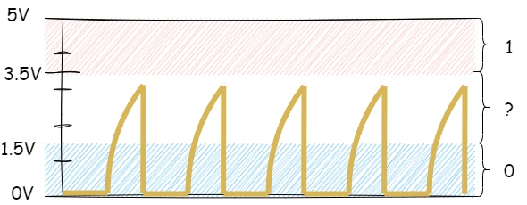
Figure 1.19 - Signal fails to reach the logical high level due to high parasitic capacitance
Due to high parasitic capacitance, the signal fails to reach the voltage level of 3.5V — the lower threshold for recognizing a logical high. One possible solution to this problem is to reduce the value of the RC constant by decreasing the resistance of the pull-up resistor.
In summary, selecting the optimal resistor value requires balancing the desired signal switching speed and minimizing power consumption. For critical applications where switching speed is a priority, lower-resistance resistors are preferred. In applications where energy efficiency is more important, higher-resistance resistors can be used, provided that this does not compromise the functionality of the circuit.
Types of Output Stages
Modern microcontrollers, as well as other ICs, offer the ability to configure their pins to operate in one of two output modes: Push-Pull or Open-Drain. This configurability provides engineers with the flexibility to select the optimal mode for each specific case, considering factors such as electrical characteristics, data exchange speed, and power consumption.
To ensure successful integration with various communication protocols connected to the microcontroller, it is essential to understand the features and operating principles of these modes.
Push-Pull Output Stage
The Push-Pull output stage consists of a pair of complementary transistors that work in harmony to actively control the voltage level on the output for both high and low states. One transistor is connected to the positive power supply, “pushing” the output signal to the high state, while the other transistor is connected to ground, “pulling” the output to the low state:
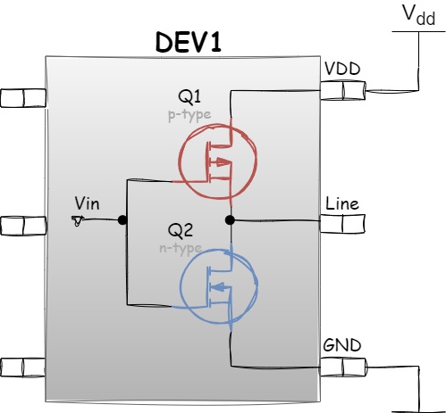
Figure 1.20 - Push-Pull Output Stage
The logic behind the Push-Pull output stage is straightforward. If the input value is logical one, the P-channel transistor Q1 is off (does not conduct current), while the N-channel transistor Q2 is on (conducts current) — resulting in the output value being logical zero, thanks to a low-impedance connection to ground:
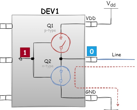
Figure 1.21 - Logical zero formation at the Push-Pull output stage
If the input value is logical zero, the P-channel transistor Q1 is on (conducts current), while the N-channel transistor Q2 is off (does not conduct current) — resulting in the output value being logical one:
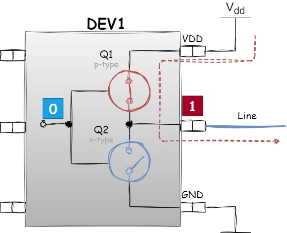
Figure 1.22 - Logical one formation at the Push-Pull output stage
Advantages
- Fast Switching: Due to active control of both levels, Push-Pull stages provide higher switching speeds compared to open-drain/collector configurations. Remember the discussion on parasitic capacitance? The speed at which any capacitance charges or discharges depends directly on the current supplied to it. In a Push-Pull design, active control of both voltage levels allows sufficient current to rapidly alter the charge of parasitic capacitance. This, in turn, increases the signal line’s operating speed.
- Lower Power Consumption: Since no external pull-up resistor is required to pull the signal to a high level, Push-Pull stages can be more energy-efficient in certain applications. The absence of a pull-up resistor eliminates quiescent current through the resistor, reducing overall power consumption.
Disadvantages
Risk of Short Circuit: If, due to a design error or failure, both transistors are turned on simultaneously, an excessive current may flow through them, potentially leading to rapid component failure and circuit damage. In a Push-Pull design, each device on the bus can actively drive the line, supplying both high and low levels. If two devices attempt to drive opposite signal levels simultaneously, this can result in a short circuit on the line. Consider the two scenarios:
- Short Circuit within the Push-Pull Stage: This occurs if both transistors are turned on (conducting current) simultaneously. This can happen during a transition in gate control voltage when one transistor has not fully turned off and still conducts current, while the other has already turned on. This effectively shorts the power supply to ground, causing a short circuit:
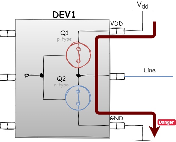
Figure 1.23 - Short circuit within the Push-Pull stage- Short Circuit across Multiple Push-Pull Stages: This occurs if two devices are on the same line, and one device attempts to drive a logical one while the other tries to drive a logical zero simultaneously. Again, this results in the power supply being shorted to ground:
Figure 1.23 - Short circuit within the Push-Pull stageComplex Control: Proper operation of a Push-Pull stage requires precise synchronization of control signals for both transistors to avoid simultaneous activation. This necessitates more sophisticated control mechanisms, complicating driver design.
Open-Drain Output Stage
The concept of an open-drain plays a key role in many digital circuits and embedded system protocols. This term refers to the way transistors are connected and operate in ICs, where the transistor’s output is not directly connected to the power supply (it remains “open”).
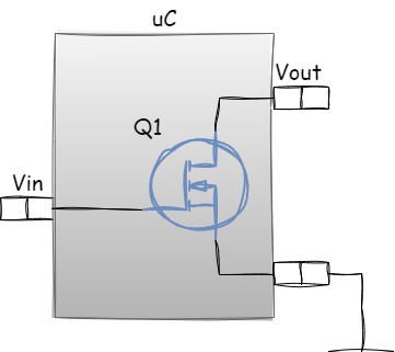
Figure 1.25 - Open-Drain Output Stage
For this circuit to operate, an external resistor is required to connect the transistor’s output to the supply voltage:
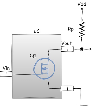
Figure 1.26 - Open-Drain Output Stage with an external resistor
When the transistor is off (does not conduct current), the output signal is formed by the pull-up resistor. This is fundamentally different from the Push-Pull configuration, where the signal is actively controlled entirely by the transistors:
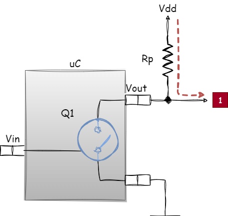
Figure 1.27 - Logical one formation at the Open-Drain output stage
When the transistor is on (conducts current), the output is connected to ground, and the output signal becomes low. No short circuits occur because the current flows through the resistor:
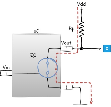
Figure 1.28 - Logical zero formation at the Open-Drain output stage
This approach to implementing a bus interface has several notable characteristics:
- The line will always remain high (logical one) unless one of the devices on the bus turns on its N-channel transistor to pull the logical level of the line down to zero. This connection type is known as “wired-AND”. More about this configuration will be discussed in the next section.
- Data transmission is effectively carried out only by pulling the line down to the value of logical zero, as the logical one is automatically set by the pull-up resistor.
- Only this configuration allows directly connecting two (or more) open-drain (or open-collector) drivers to a single bus: the pull-up resistor ensures there is no short circuit between Vdd and GND.
Wired AND Connection
In wired embedded protocols, it is common to encounter situations where devices are connected to a shared line pulled up to the supply voltage through a pull-up resistor:
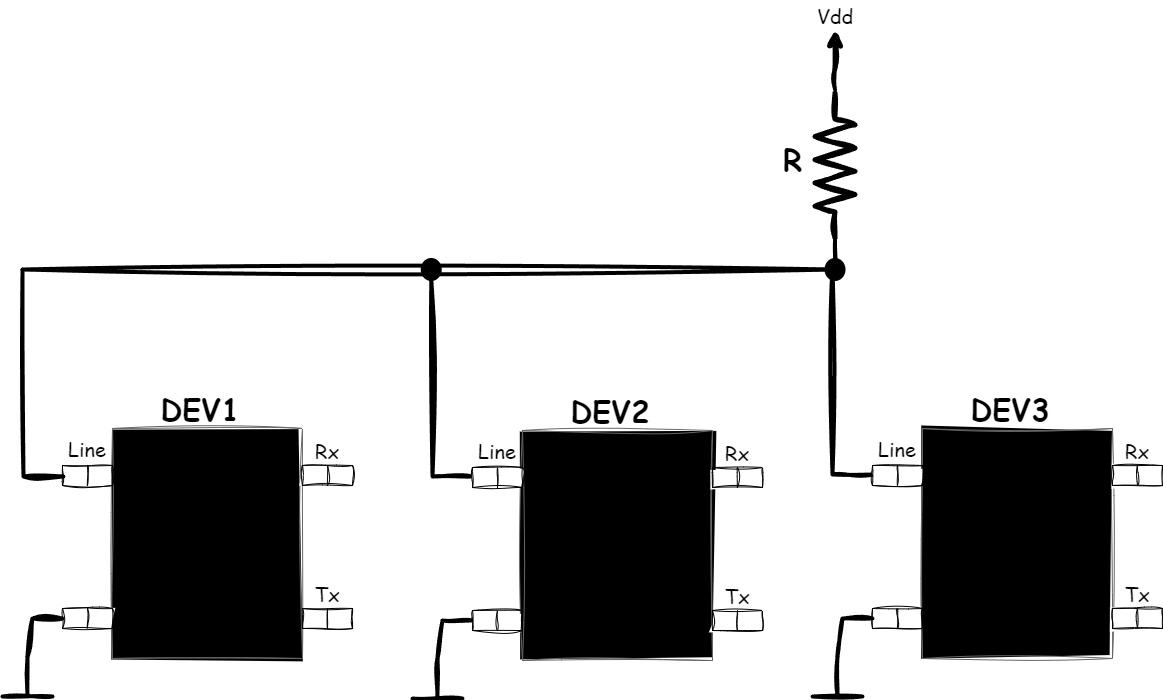
Figure 1.29 - Wired AND Connection
This type of connection is used in protocols such as 1-Wire, I2C, and I3C and is called Wired AND because, just like the result of a logical AND operation is zero if at least one operand is zero, in the Wired AND connection, the line will be in a logical one state if all devices on the line drive it to a logical one, and in a logical zero state if at least one device drives it to a logical zero.
The truth table for the diagram:
| DEV1 | DEV2 | DEV3 | BUS |
|---|---|---|---|
| 0 | 0 | 1 | 0 |
| 0 | 0 | 0 | 0 |
| 0 | 1 | 1 | 0 |
| 0 | 1 | 0 | 0 |
| 1 | 0 | 0 | 0 |
| 1 | 0 | 1 | 0 |
| 1 | 1 | 0 | 0 |
| 1 | 1 | 1 | 1 |
This behavior is enabled by the fact that the output stages of all devices connected to the shared line are implemented as Open-Drain:
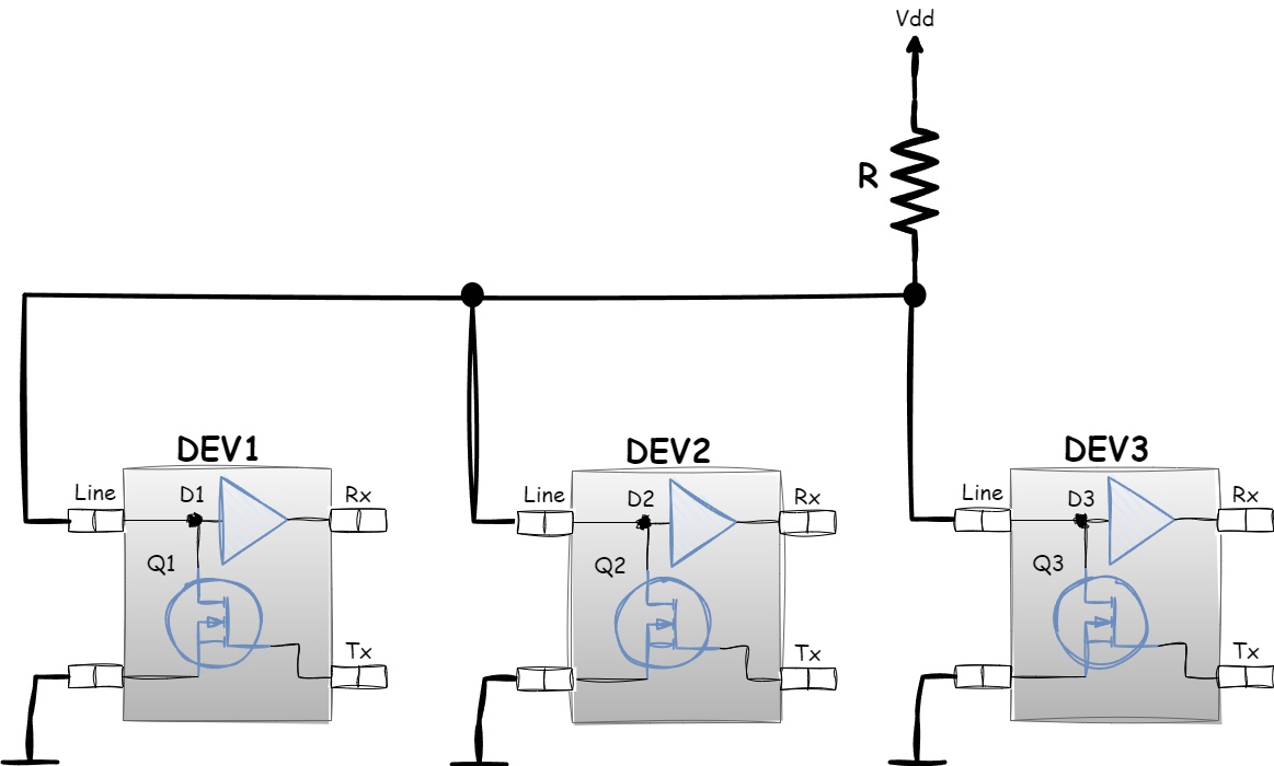
Figure 1.30 - Output stages of devices in a Wired AND connection
As you can see, all devices connected to the shared line use Open-Drain output stages: Q1, Q2, and Q3. Input buffers D1, D2, and D3 allow the devices to also read the line state.
Let’s examine how the Wired AND connection works.
As we recall from the section Open-Drain Output Stage, an Open-Drain stage actively drives only the low level, while the high level is set automatically by the pull-up resistor. Thus, when all output transistors of the devices connected to the bus are off, the entire line is pulled to the supply voltage by the pull-up resistor, resulting in a logical one state:
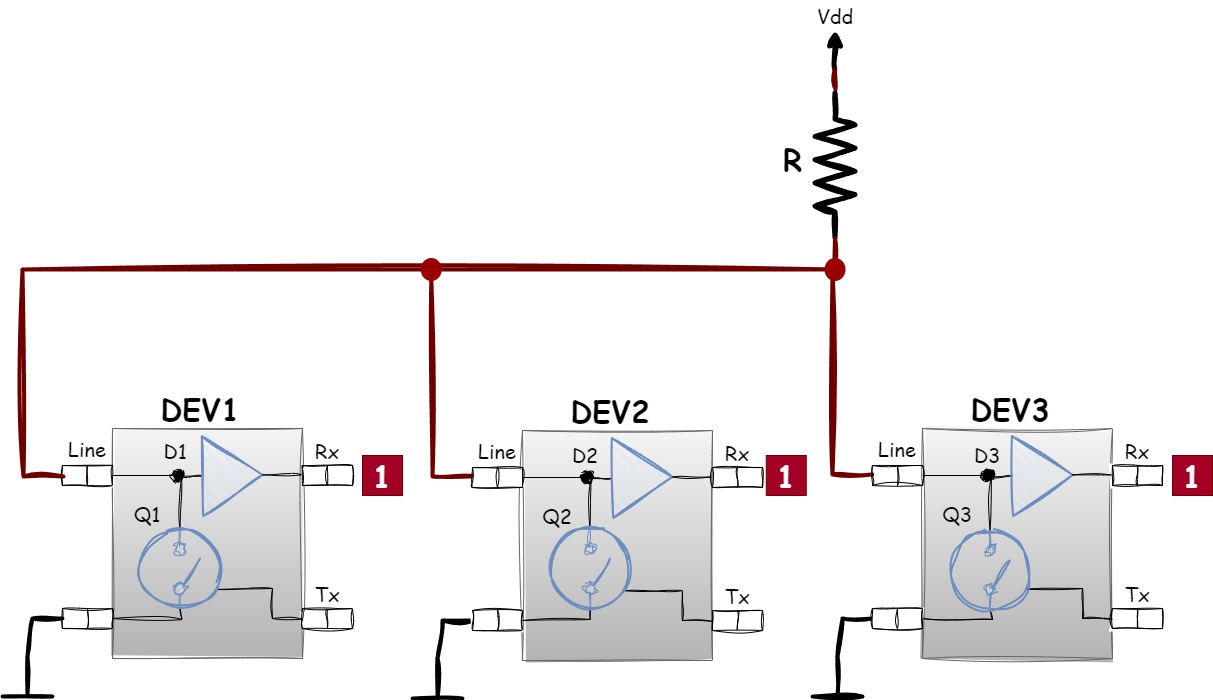
Figure 1.31 - Logical one formation in a Wired AND connection
Now let’s see what happens if, for example, device DEV2 turns on its transistor Q2:
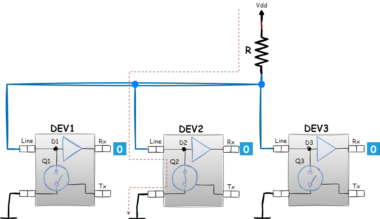
Figure 1.32 - Logical zero formation in a Wired AND connection
In this case, the entire line transitions to a low logical state because device DEV2 effectively pulls the line to ground through its active transistor Q2. Notably, devices DEV1 and DEV3 do not change their states and effectively “want” to set a logical one on the line. However, it only takes one device (DEV2 in this case) setting the line to a logical zero for the line to adopt a logical zero state. This is why the bit 0 is called dominant.
This feature of the Wired AND connection underpins fundamental functions in various protocols, such as the device discovery algorithm in the 1-Wire bus and bus arbitration in I2C, which will be discussed in their respective chapters. Moreover, thanks to the use of Open-Drain stages, this connection is safe for operation with multiple devices on the same line, regardless of whether any device is transmitting a logical one or zero. These unique characteristics make the Wired AND connection widely used in many wired communication protocols.
Conclusion
Communication protocols are the foundation of digital systems, enabling the transmission and processing of information in binary form. In this chapter, we explored the key aspects underlying such protocols, from the concepts of logical one and logical zero to practical implementations, including various voltage levels, resistor usage, types of output stages, and device connection methods.
Understanding how data transmission works at the physical level is critical for designing and configuring wired protocols. Knowledge of which voltage levels correspond to logical values, how to select appropriate resistor values, and the characteristics of different output stages is essential for proper design and ensuring reliable data transmission.
Each of these factors can significantly impact system efficiency, noise immunity, and compatibility with various devices. Engineers and developers must consider these details when designing digital interfaces, enabling the creation of more robust and high-speed communication systems.
Further exploration of specific wired protocols, such as 1-Wire, UART, I2C, SPI, and others, will reveal even more details to consider when developing effective and reliable solutions for digital data transmission.
Stay in touch with us
Stay tuned to this blog or follow us on LinkedIn and Twitter @PlatformIO_Org to keep up to date with the latest news, articles and tips!